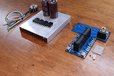
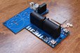
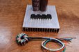
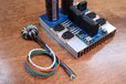
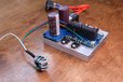
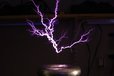
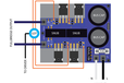
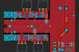
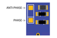
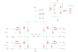
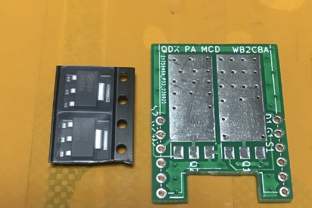
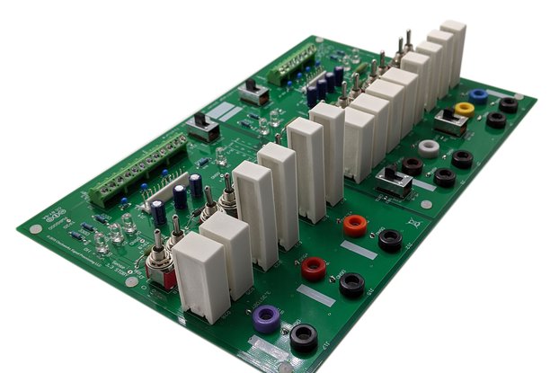
TO-247 Full-bridge with full wave voltage doubled capacitor bank. A fully integrated High Side for SSTCs, DRSSTCs, and HV sources
Designed by WaskaLabs Designs in United States of AmericaThis product is no longer available for sale.
The seller may be offering an improved version or it may be hanging out on the beach, enjoying the retired life.
The full-bridge bus 2.0 is a fully integrated "high side" system designed for SSTC and DRSSTC Tesla coils and other high power inverter applications. For assembly pictures and information - check out…
Read More…The full-bridge bus 2.0 is a fully integrated "high side" system designed for SSTC and DRSSTC Tesla coils and other high power inverter applications. For assembly pictures and information - check out the WaslaLabs Github repo for the project.
If you would like a fully assembled kit ready to go out of the box, message me directly. Lead times and cost depend on part availability and design specifications.
Finished System Specs:
Basic Kit comes with:
Required - available as addon:
Required - Not included:
IGBT and MOSFET recommendations:
Rectifier & Bus:
The voltage doubler configuration doubles the peak-to-peak voltages seen on the AC input. For example, US mains is 110V RMS, but ~170Vpp. So if US mains is connected directly to the input, it should charge the capacitor bank to ~340V. The capacitors on the bus are connected in series, so each capacitor should be rated to hold the full Vpp of the mains input (in the US, I like to use 250V). It is highly advisable to spec these caps to handle ~30% more than the voltage you expect to see in them, so a 500V total cap charged to 340V is a safe bet. In 220V land, you will want to use 450V capacitors for a total of 900V. Bare in mind that the total capacitance of the bus will decrease by half as the voltage doubles. So two 250V 1000uF caps in series will give you 500V at 500uF. This should be kept in consideration when designing the system.
Recommendations:
If you plan to modify the board to a standard rectified voltage, spec your caps accordingly. I would suggest ~150V caps for US mains (300V total rating), doubling it for 220V mains, at the highest uF you can get in the correct footprint to fit the PCB.
The KBU-1010 bridge rectifier is rated for 10A continuous and 300A surge. If you plan to run high currents monitor the temperature of the rectifier and add a heatsink if needed. The fuse is a 6x20 glass cylindrical type which are standard and available cheap online or locally at hardware stores.
Inverter & Gates:
The inverter portion is pretty straightforward. The switches (IGBTs or MOSFETs) are connected directly to the heatsink with a silicone heat pad (sil pad) to electrically isolate the switches from the heatsink (Very important!). The pins of the switches should be bent upwards before mounting, then bent to contact the pads and soldered in place. Removal can be done with a soldering iron, but the simple solution is to use hot air to heat the pads. It is easier to do this after unscrewing the switches from the heatsink, otherwise you may not be able to disconnect it easily. The leads can also be clipped first if this becomes an issue.
The Gate Drive Transformer (GDT, typically 1:1:1:1:1) should be wound and phased. The secondary windings of the GDT should be soldered directly to the pads with the phase wires soldered to the pads with silkscreen around them, and the anti-phase ends soldered to the other pad. Make sure to wind the GDT with enough extra wire to make it easy to mount (I like to mount them to the side of the heatsink). One important note is that the GDT secondaries should ALL BE LENGTH MATCHED to avoid skew in the timing between the switches.
The gate components are not one size fits all. The gates and waveforms should be thoroughly tested to assure the switching waveform is correct. If it isn't, you may need to change gate resistors and remove the diodes, etc. until you can get it right. The TVS diodes are SMAJ26 26V TVS which is designed for up to 24V drive voltages. If using lower voltages you may want to change the value of the TVS. Tuning gates is not in the scope of this document, but it is an art and takes some time to get right. But having a proper driver, GDT, gate components, and the right switches are important in getting this right. A good resource for this is Ritchie Burnett's GDT waveform troubleshooting guide.
Step by Step Assembly:
Testing Gates:
Testing Inverter:
Troubleshooting:
This design is meant to be configurable and modular to be able to fit many topologies. There are far too many variations in application, drive methods, and use cases for me to be able to help in the debugging. If you have issues getting it to work, do your research and read up on forums. I have provided schematics and resource information on the system so that you have all information necessary to figure out the issue. But standard troubleshooting like adding/removing components and thinking through the design will be the only way to get it running. I am happy to help when I can, but ultimately what you build with this cannot be fixed IT style.
$195.00
Free Shipping!
$5.00
Free Shipping!
$140.00
Free Shipping!
$4.95
Free Shipping!
By clicking Register, you confirm that you accept our Terms & Conditions
We recognize our top users by making them a Tindarian. Tindarians have access to secret & unreleased features.
We look for the most active & best members of the Tindie community, and invite them to join. There isn't a selection process or form to fill out. The only way to become a Tindarian is by being a nice & active member of the Tindie community!